
Syenta raises Series A from Playground Global and Australia’s National Reconstruction Fund to scale semiconductor innovation; Pat Gelsinger (Ex-CEO of Intel) joins the board.
Syenta, a next-generation semiconductor company building advanced packaging technology for AI systems, has raised A$37 million (US$26 million) in Series A funding led by Playground Global and Australia’s National Reconstruction Fund (NRF), with participation from Investible, Salus Ventures, Jelix Ventures and Wollemi Capital.
The raise brings total funding to date to A$51.1 million (US$36.4 million), reflecting continued support from leading Australian and global investors as Syenta moves toward commercialisation.
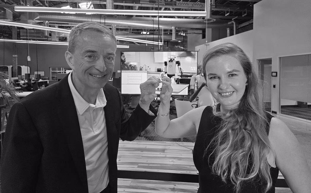
As part of the round, Pat Gelsinger, General Partner at Playground Global and former Chief Executive Officer of Intel, will join Syenta’s Board of Directors, adding deep semiconductor leadership at a time when AI system scaling is increasingly constrained by interconnect and packaging limitations rather than compute alone.
Playground Global’s investment also supports Syenta’s international expansion, including the establishment of US operations in Arizona. NRF’s investment is directed toward strengthening advanced semiconductor manufacturing capability in Australia.
AI scaling is hitting a new constraint layer
As AI systems scale, the limiting factor is increasingly determined by how efficiently chips connect and communicate, rather than compute.
Interconnect bandwidth, packaging density and system-level communication between chips have become central constraints in performance scaling. These challenges sit within advanced packaging, where manufacturing complexity and physical limits are becoming defining bottlenecks for next-generation AI hardware.
At the same time, advanced packaging capacity - the manufacturing step where chips are connected to memory and to each other- remains concentrated in a small number of specialised facilities globally, creating structural supply chain constraints across the semiconductor industry.
A manufacturing approach built for scale
Syenta’s Localized Electrochemical Manufacturing (LEM) technology enables high-density chip-to-chip interconnects within existing semiconductor manufacturing infrastructure.
Early results show micron-scale interconnects and measurable efficiency improvements, including:
- Up to 40% fewer process steps
- No redesign required for existing fabrication infrastructure
- Higher interconnect density enabling improved bandwidth between chips
By working within established manufacturing environments rather than replacing them, LEM is designed to improve scalability in advanced packaging and reduce pressure on constrained global supply chains. The process has been validated through industry programs, including collaborations with leading semiconductor equipment providers.
Playground Global backs the next scaling inflection point
“This is a new way of building high-performance systems at unprecedented scale and power, particularly as AI workloads continue to grow,” said Pat Gelsinger, General Partner at Playground Global.
“AI’s next scaling challenge isn’t just compute — it’s how chips connect. Syenta is addressing a fundamental constraint in advanced packaging, and that has the potential to reshape how future systems are built and scaled.”
Playground Global led the round, underscoring conviction in Syenta’s approach to enabling the next phase of AI infrastructure globally, including its expansion into the United States.
NRF backing focused on Australian manufacturing capability
“Syenta exemplifies the type of globally competitive, high-impact innovation the NRF was created to support,” said Dr Mary Manning, Chief Investment Officer at the NRF.
“By advancing next-generation packaging technologies, Syenta strengthens Australia’s role in critical supply chains while contributing to global semiconductor resilience.”
NRF’s support is focused on strengthening advanced semiconductor manufacturing capability within Australia, particularly in technologies that can scale into global supply chains.
Why advanced packaging is now the bottleneck
Across the semiconductor industry, advanced packaging is increasingly recognised as a key constraint in scaling AI systems.
As architectures move toward heterogeneous, chiplet-based designs, performance depends on significantly increasing interconnect bandwidth while maintaining power efficiency and manufacturability.
“AI is driving unprecedented demand for heterogeneous, panel-scale systems. These systems — often composed of hundreds of chiplets — require continued innovation in packaging architectures to increase interconnect bandwidth while improving energy efficiency,” said Deepak Kulkarni, Senior Fellow at AMD.
Expanding into the United States
As part of its commercialisation strategy, Syenta is establishing a presence in Arizona, positioning the company closer to leading semiconductor customers and advanced packaging ecosystems.
The expansion is supported by Playground Global and is designed to accelerate collaboration with global manufacturing partners, while strengthening supply chain resilience across both the United States and Australia as AI infrastructure demand continues to grow.
About Syenta
Syenta is a semiconductor technology company headquartered in Sydney, Australia. The company was founded on research from the Australian National University and has developed Localised Electrochemical Manufacturing (LEM), a process technology for high-density chip-to-chip interconnects in advanced semiconductor packaging.

Syenta has been featured in Forbes - revolutionizing chip packaging, breaking the AI memory wall, and powering faster, smarter AI and High Performance Computing (HPC) worldwide.
Syenta has advanced to the Semi-Finals of the 2025 SEMI Startups for Sustainable Semiconductors (S3) Program. We're honoured to be among 35 selected from a record pool, showcasing our LEM technology for efficient, sustainable electronics manufacturing.
.webp)