
Breaking the AI memory wall through ultra-high bandwidth High-Resolution Interconnects
Syenta’s breakthrough


We’ve developed a new fabrication method
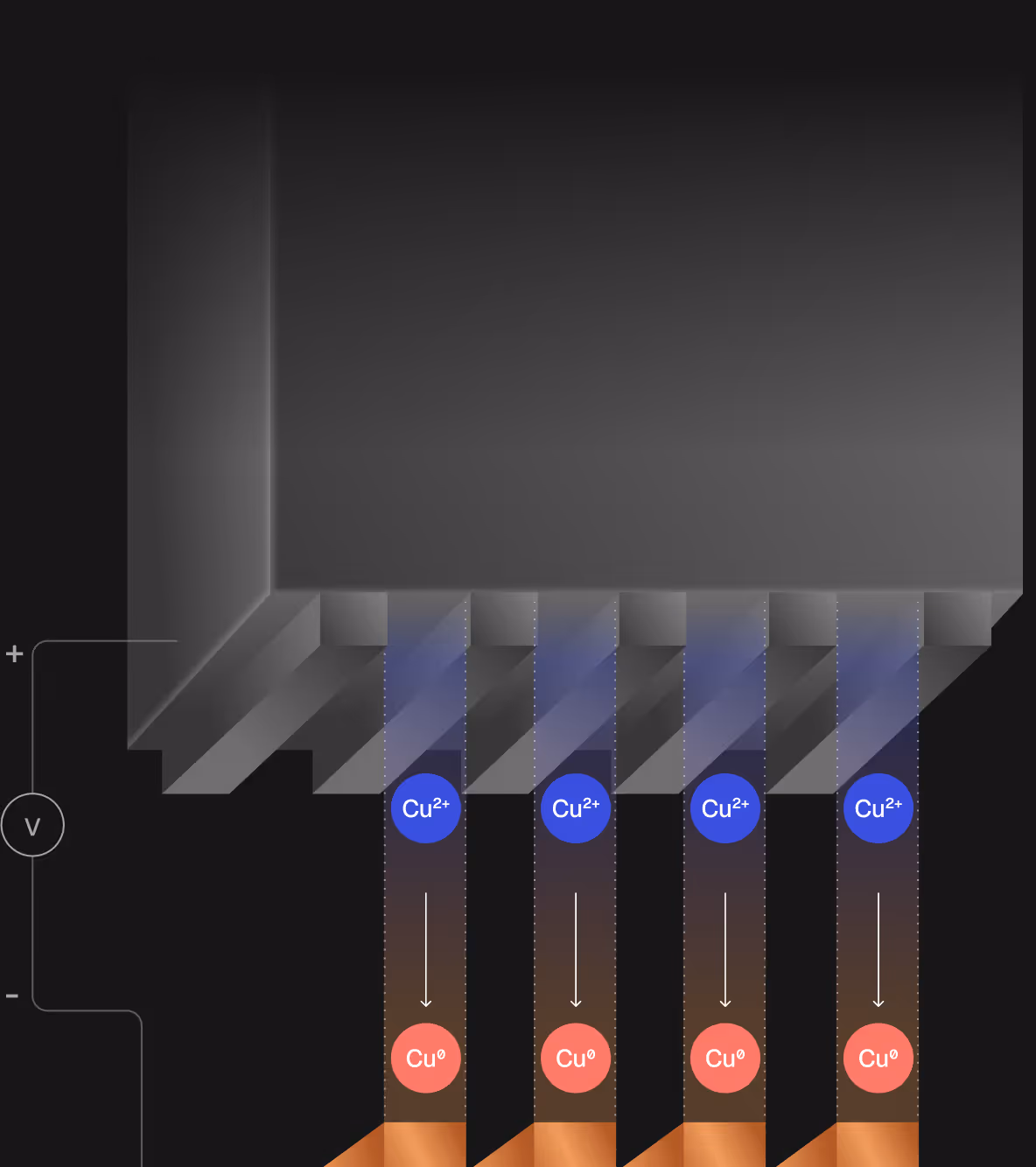
Three axes of scaling through Syenta’s technology
Scale down
Scale out
Scale up
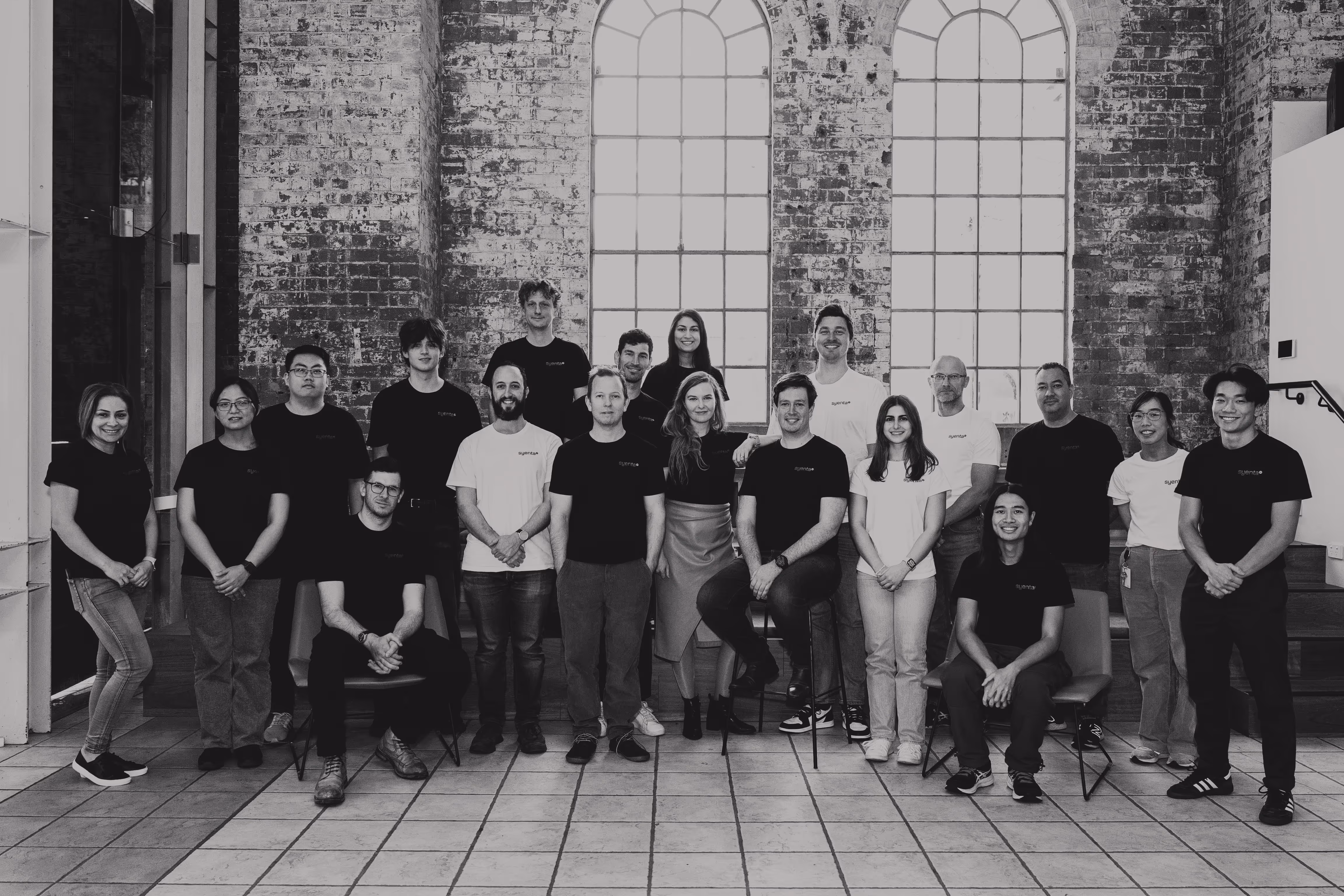
Leadership
.avif)
.avif)
.avif)
.avif)
.avif)
.avif)
.avif)
.avif)


%201.svg)


Syenta has been featured in Forbes - revolutionizing chip packaging, breaking the AI memory wall, and powering faster, smarter AI and High Performance Computing (HPC) worldwide.
Syenta has advanced to the Semi-Finals of the 2025 SEMI Startups for Sustainable Semiconductors (S3) Program. We're honoured to be among 35 selected from a record pool, showcasing our LEM technology for efficient, sustainable electronics manufacturing.
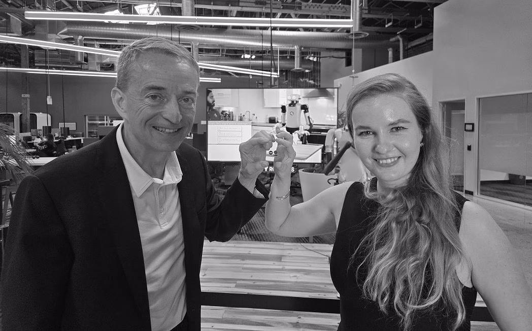
Syenta had a strong presence at the 3D & Systems Summit 2025 in Dresden! CEO Jekaterina Viktorova and BD Head Sebastiaan Muller showcased our LEM tech and connected with global leaders in 3D integration. Thanks to Steffen Kröhnert for the kind invitation to speak.
We’re excited to share that 3D InCites has featured Syenta - Breaking AI’s Memory Wall with Next-Gen Chip Packaging Technology. Syenta's proprietary Localized Electrochemical Manufacturing (LEM) technology enables micron-scale resolution in advanced semiconductor packaging, offering a scalable solution to the pressing memory bandwidth bottlenecks in AI computing.
.avif)
Syenta in the US! We showcased our Localised Electrochemical Manufacturing (LEM) tech at SPIE and IMAPS DPC 2025, with presentations by CTO Ben Wilkinson and Head of Sales Sebastiaan Muller. LEM enables precise, scalable metal deposition across advanced applications.
.webp)