
Breaking the AI memory wall through ultra-high bandwidth High-Resolution Interconnects
Syenta is architecting the future of AI computing through its revolutionary Localized Electrochemical Manufacturing (LEM) technology, which enables High-Resolution Interconnects -a new class of chip-to-chip connections that transcends traditional packaging to deliver wafer-level system integration at unprecedented density.
Syenta’s breakthrough
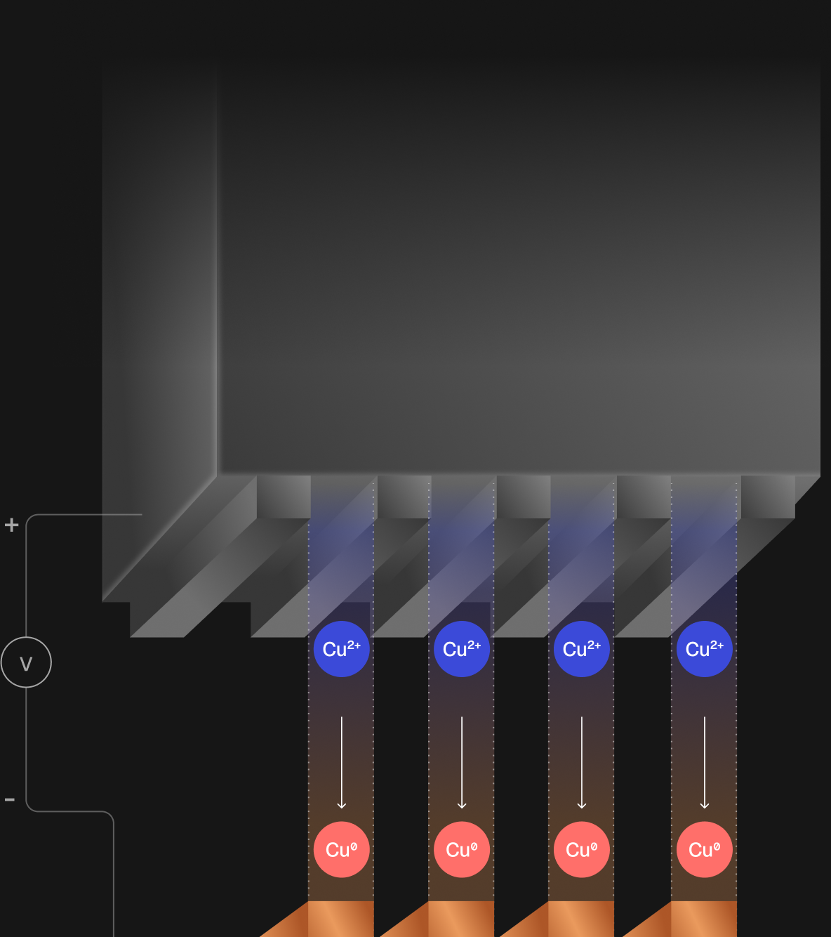
With Syenta’s interconnect technology the compute-memory interface is no longer the bottleneck for AI. Our interconnects are sub-micron; manufactured on large >1000 mm2 packages, and the process has 3x the throughput of existing fabs.


We’ve developed a new fabrication method
Localized Electrochemical Manufacturing combines deposition and patterning into a single step. It uses a stamp electrode with a dielectric pattern that defines localized electrochemical cells, enabling precision metal deposition only within those cells.
Three axes of scaling through Syenta’s technology
Scale down
Increase bandwidth, <=1/1 µm RDL
Scale out
Expand package size, 510/600 mm Panel
100-200mm field size
Scale up
High-volume production 3x the productivity of current manufacturing technologies
Leadership
.webp)
Dr. Jekaterina Viktorova
CEO, co-founder
Dr. Jekaterina Viktorova
CEO, co-founder
.webp)
Ben Wilkinson
CtO, co-founder
Ben Wilkinson
CtO, co-founder
.webp)
Prof Luke Connal
CSO, co-founder
Prof Luke Connal
CSO, co-founder
.webp)
Zachary Dowse
COO, co-founder
Zachary Dowse
COO, co-founder
.webp)
John McClure
CIO
John McClure
CIO

John Ghekiere
VP engineering
John Ghekiere
VP engineering
.webp)
Sebastiaan Muller
Head OF BD
Sebastiaan Muller
Head OF BD
.webp)
Niki Scevak
Board director
Niki Scevak
Board director
investors & partners


%201.svg)


.webp)

.webp)